
Time: 2023.12.18
At the recent IEDM, Samsung Electronics (hereinafter referred to as Samsung) announced technology beyond the limits of DRAM miniaturization at the earlier IEDN. Micron Technology (hereinafter referred to as Micron) and TSMC will announce technologies to increase the capacity of non-volatile memory.
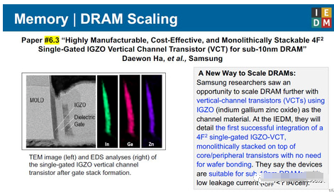
Samsung Electronics said it has developed vertical channel DRAM cell transistor technology suitable for technology nodes below 10 nanometers. The oxide semiconductor IGZO is used as the channel material. The vertical channel transistors used in DRAM cells are monolithically integrated on the circuit transistor layer and the peripheral circuit transistor layer.
Micron Technology has prototyped a 32Gbit large-capacity non-volatile RAM, which is composed of two stacked array layers of ferroelectric memory cells (1T1C type). Storage density is increased by stacking arrays of memory cells on top of a CMOS peripheral circuit area.
TSMC has developed an embedded memory in which the STT-MRAM cell is configured with a selector and a magnetic tunnel junction (MTJ), and the cell array is arranged at the intersection. Prototype memory cell arrays using 16nm and fine processing technologies.
Interestingly, the memory technologies developed by Samsung and Micron both achieve storage density by placing memory cell array layers on top of peripheral circuit layers. Both companies have experience mass-producing 3D NAND flash memory using similar technology (CMOS under array). On the R&D front, there are signs of expansion beyond flash into high-density memory.
Samsung: Promoting DRAM and moving forward
Earlier this year, Samsung posted a blog saying that this year is particularly meaningful for Samsung because it marks its 30th anniversary as a large DRAM supplier, a record that dates back to 1992 when Samsung developed 64Mb DRAM.
Over the next few years, Samsung will continue to produce quality DRAM through disruptive innovation and scaling technological advancements.
Samsung says DRAM expansion has never been more difficult. However, Samsung is already preparing solutions to overcome the challenges faced by DRAM.
As the size of DRAM drops to about 10nm, the process difficulty increases significantly. The smaller the dimensions, the greater the challenges posed by patterning, cell transistors, cell capacitance and bandwidth requirements. To overcome these challenges, Samsung has been preparing its own miniaturization process and equipment technology. It has also been exploring and developing disruptive solutions in new materials and new array architectures.
Samsung’s shrinking process will continue to evolve, driving progress on its DRAM roadmap. EUV patterning will continue to advance due to High-NA, which will allow Samsung to enhance its patterning capabilities with smaller process steps. In addition, new metals with lower resistance will be introduced to shrink word lines and bit lines.
The use of these new materials can increase the word line and bit line resistance by 40% and 35% respectively. This enables these key technologies to push the limits of battery size.
Dielectrics with higher k values and high aspect ratio contact etch processes are also critical to ushering in the next phase of DRAM capacitors. Samsung is ready for this, too, and is fully capable of atomically controlling the crystallinity of high-k dielectrics at the subnanometer scale. Using FinFETs, Samsung can increase speed and power by 30% and 20% respectively at 0.9V operating voltage.
What you see here is Samsung's DRAM product, which will be released starting next year. These include Samsung's high-capacity 32Gb DDR5 for data centers and servers, which will support modules up to 1TB. Its low-power mobile DRAM and high-performance graphics DRAM will feature speeds of 8.5Gbps and 28Gbps respectively, making them the fastest in the world. LLW DRAM, a low-latency wide IO product, and HBM offering ultra-high bandwidth of 1TB/s are also in development.
Samsung also offers a wide range of custom DRAM solutions, covering everything from cache to high-capacity memory. These include LLC-DRAM, a last-level cache DRAM; HBM-PIM, a high-bandwidth memory with in-memory processing; AXDIMM, a DIMM with embedded near-data processing; CXL-MXP, a memory expander; and CXL-PNM, a Expander for new CXL interface processing capabilities.
With an eye on the future, Samsung continues to explore the next steps in DRAM technology and develop the solutions needed to realize this future. With innovations from traditional DRAM to custom DRAM, Samsung is ready to deliver the DRAM solutions the industry demands. It will continue to innovate, convinced that the way forward lies in accepting more challenges, innovation and collaboration.